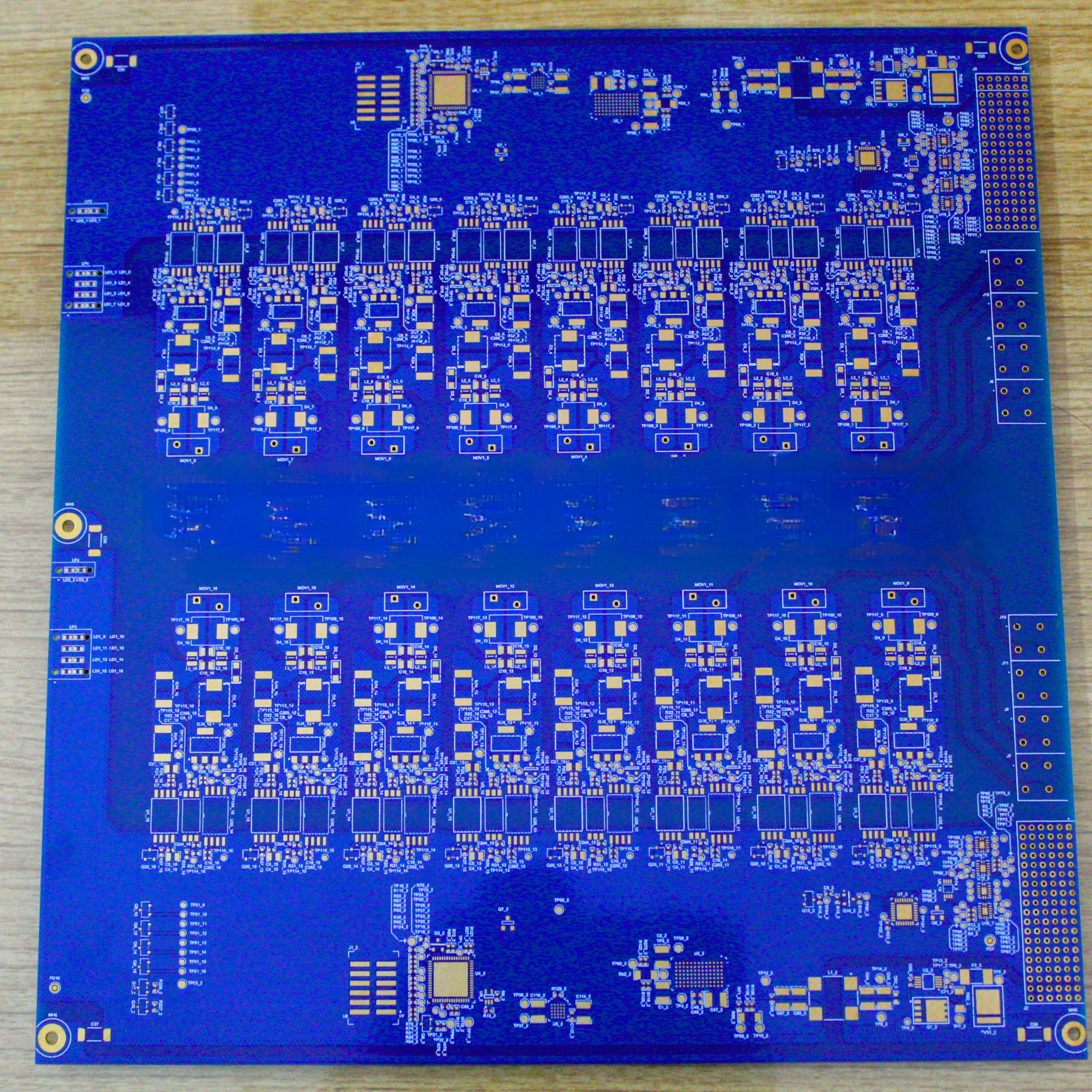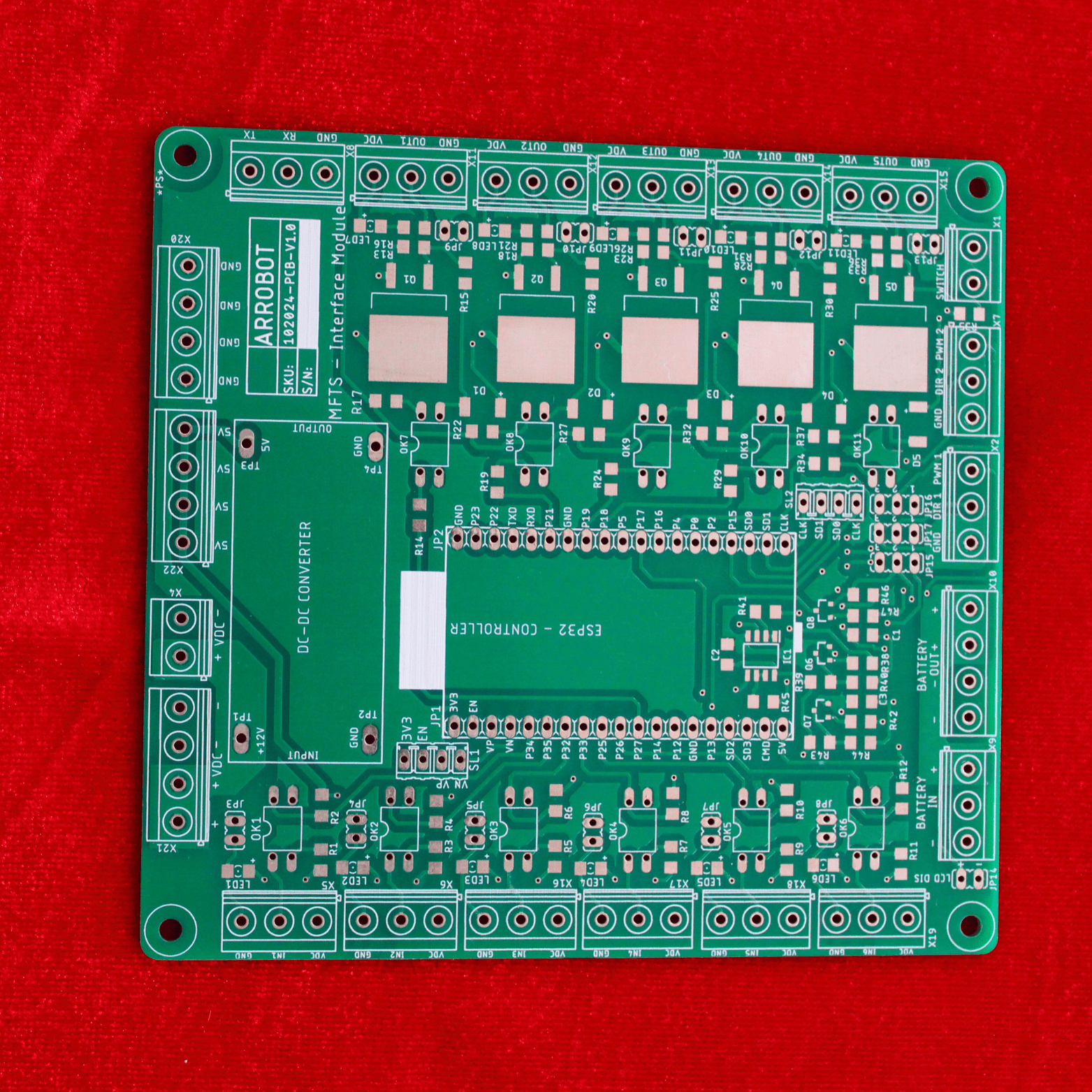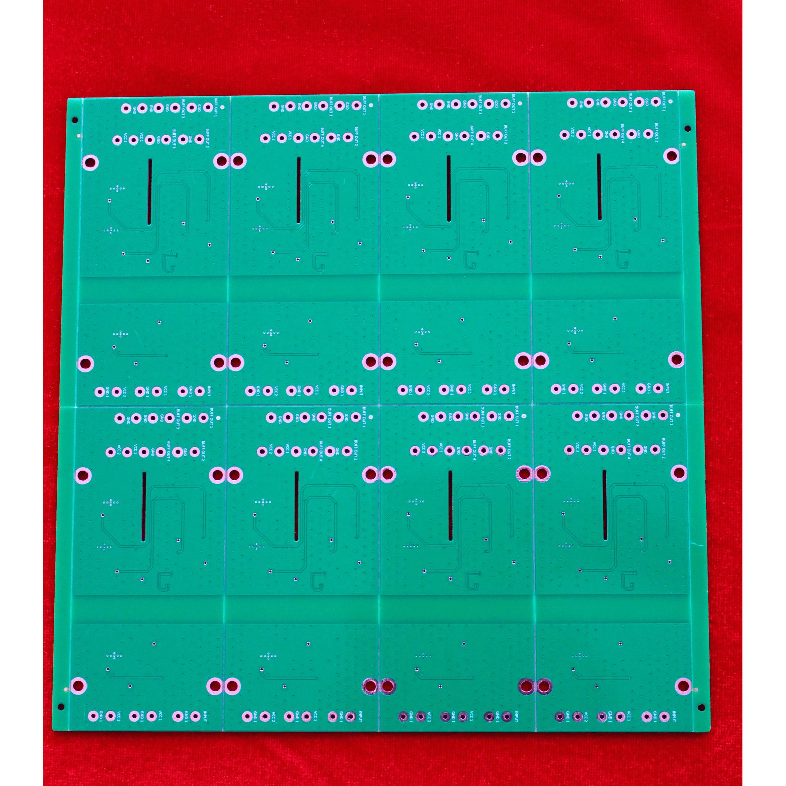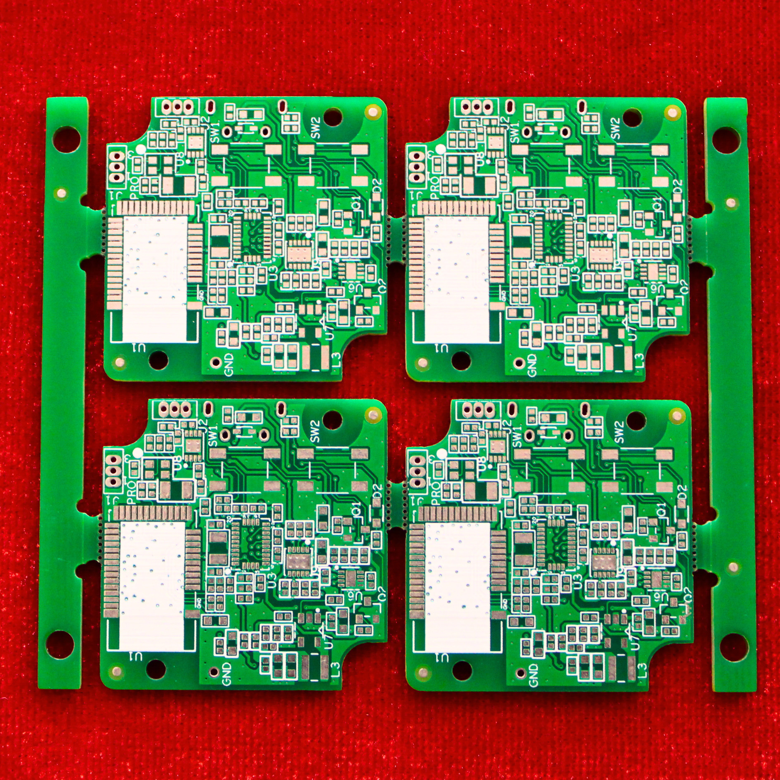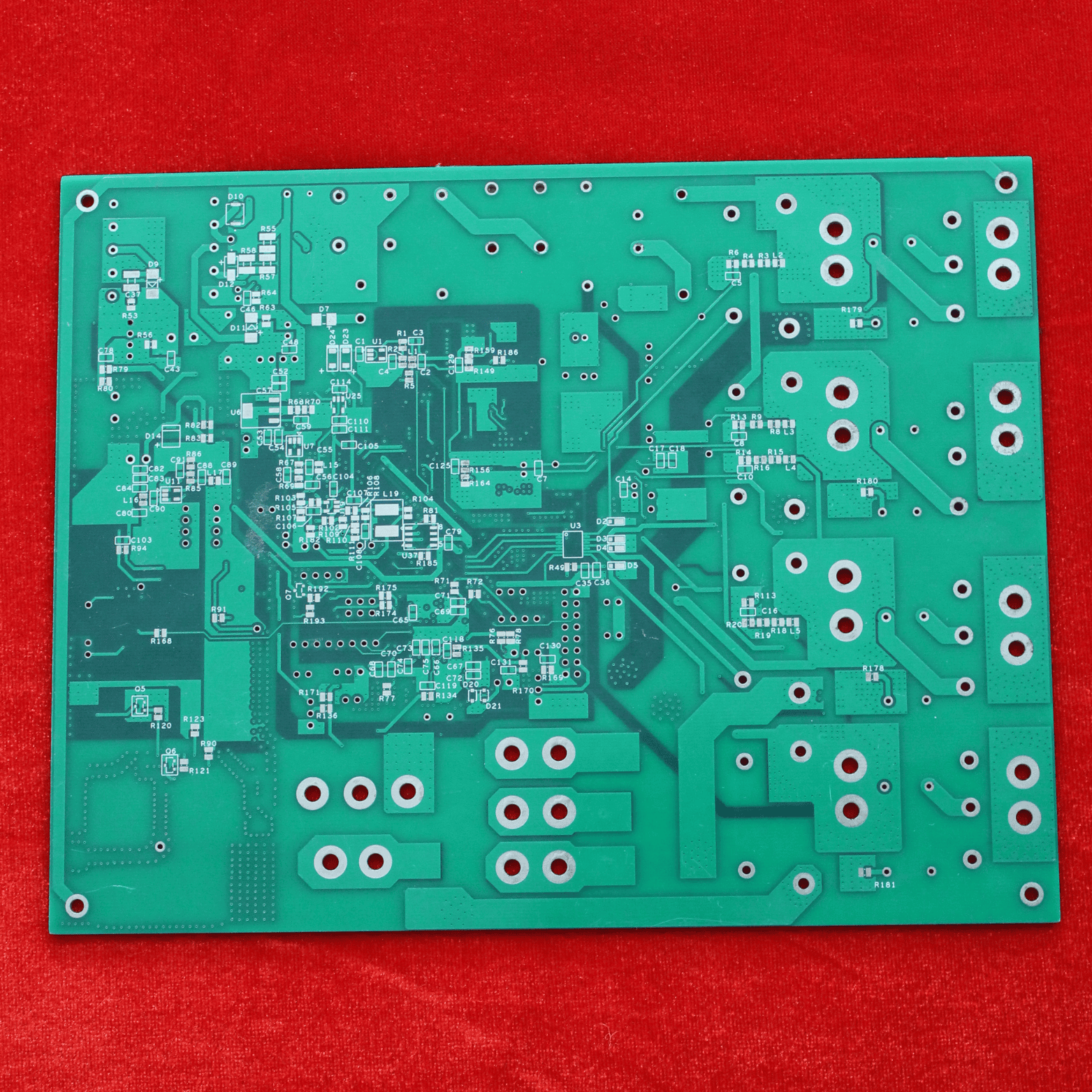
PCB Fabrication
At Glonix Electronics Pvt Ltd, we provide high-quality PCB fabrication services that bring your designs to life. From prototypes to large-scale production, our boards are engineered for precision, reliability, and performance.
Our Capabilities
Board Types – Single, Double, and Multilayer PCBs (up to 24 Layers)
Materials – FR4, Aluminum (MCPCB), Rogers, Polyimide, Flex & Rigid-Flex.
Surface Finishes – HASL, Lead-Free HASL, ENIG, OSP, Immersion Silver.
Advanced Features – Controlled impedance, gold fingers, edge plating, V-cut & slots.
Specifications – Track/Spacing: 4/4 mil, Min hole size: 0.2 mm, Copper thickness: 1oz–3oz.
Why Choose Us
✅ Strict quality control with electrical testing & inspection.
✅ Fast prototyping to mass production flexibility.
✅ Cost-efficient solutions without compromising quality.
✅ Complete integration with our PCB design and assembly services.
Ready to fabricate your PCB?
Send us your Gerber files today for a quick and competitive quotation
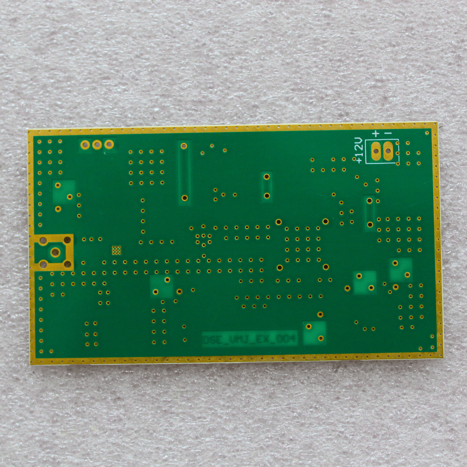
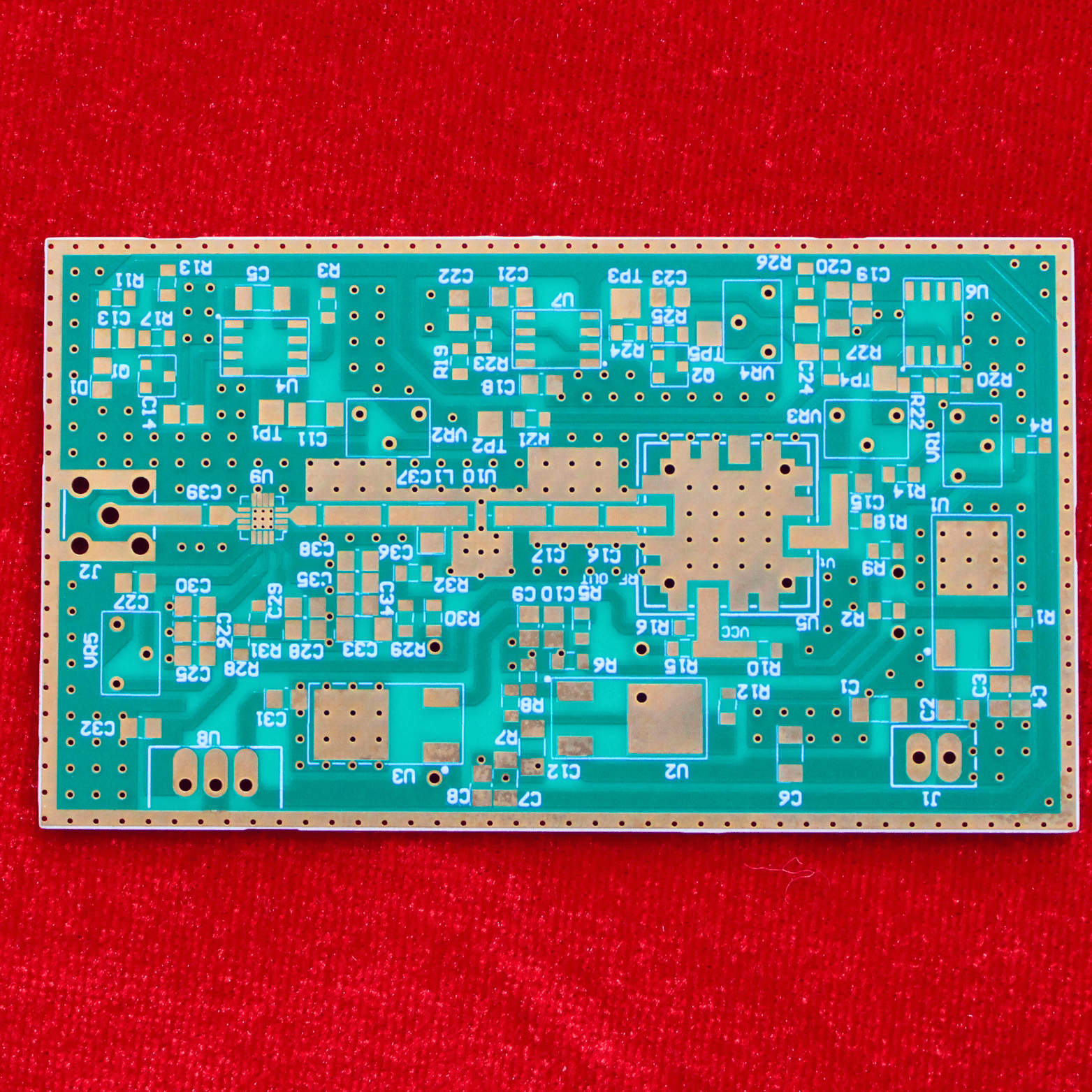
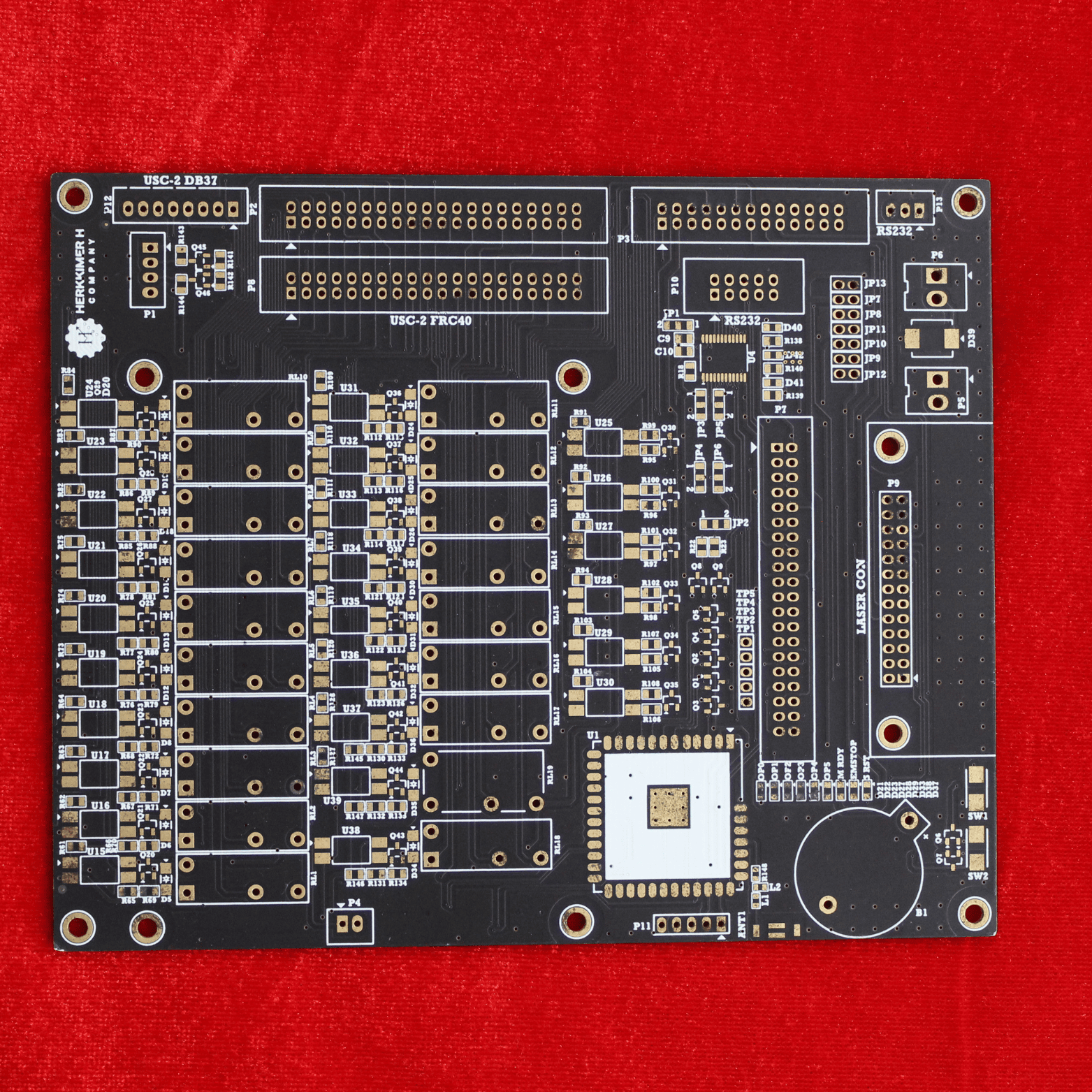
Our Product Demo