PCB DESIGN AND TRAINING WORKSHOP
Printed circuit board (PCB) design brings your electronic circuits to life in the physical form. Using layout software, the PCB design process combines component placement and routing to define electrical connectivity on a manufactured circuit board.
PCB Design is considered as one of the most important fields in electronic industry & every electrical/electronics engineer should have some basic knowledge in this domain.
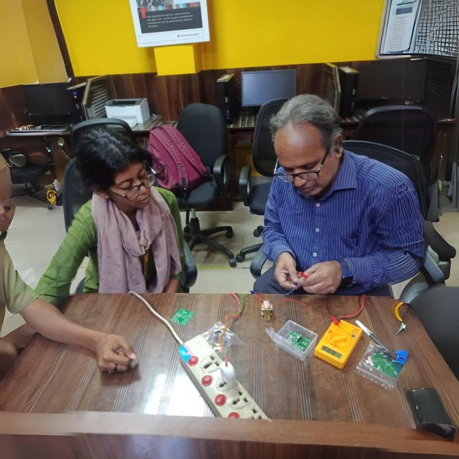
GLONIX Electronics provides end to end training in PCB Design Course at an AFFORDABLE FEE which is customized as per each candidate's requirement of modules and content.
Electronic design automation (EDA), also referred. to as electronic computer-aided-design (ECAD), is a category of software tools for designing electronic system such as integrated circuit and printed circuit boards. We provide basic knowledge about electronic circuits, hands-on experience on OrCAD software tool & basics of PCB manufacturing, Component Procurement, Assembling & Stencil.
OrCAD Capture is a schematic capture application, and part of the OrCAD circuit design suite... Capture includes a component information system (CIS), that links component package footprint data or simulation behaviour data, with the circuit symbol in the schematic.
SOFTWARE OVERVIEW
CAPTURE
- Project Creation
- Library Part Creation
- BoM Generation
- Export. Pdf
- Pad Preation
- Footprint Creation
- Component Placement
- Routing, Art work creation, Drill file Creation
- Gerber Creation
PCB Design Training includes the Study Materials, Software, Course Completion Certificate, Project guidance & Assistance.